
Field programmable gate arrays, or FPGAs are wonderful little devices. In a nutshell, they are a whole load of logic blocks, wired together with interconnects. These logic blocks can be wired up however you like, to create simple, or complicated circuits. Anything from a simple XOR gate, to a CPU, to an entire system (if you have enough money to buy the biggest ones). Think of them as a big box of lego bricks that you can combine in any way you want to create any kind of digital circuit.
FPGAs have been used in many applications - emulation of older systems being one. The MiSTer is one such example. Jeri Ellsworth's C-One is another. But really, FPGAs are found everywhere. They are quick, robust and adaptable to most situations.
My friend Will runs the Project-F website where he investigates all things FPGA. I've been helping out by building some boards for us, and this is one of the first. I'd like to show you all how I went about building one of our early prototypes, the triumphs and pitfalls and hopefully inspire folks to give it a go themselves.
For this prototype, we've been using the Spartan 7 Series of FPGAs from Xilinx. Their XC7S6 model is the cheapest with 6,000 logic cells and 100 I/O pins to play with. The FTGB196 version has a 1mm ball pitch and is 15mm square. This is good as it's large enough to handle easily. Any smaller and I'd have trouble soldering it up.
FPGAs take quite a number of different voltages. In our design, we are running the I/O at 3.3V (as that's fairly standard for hobbyists), but we also need to provide 5V, 1.8V and 1.0V. That's 4 different voltages we need to deal with! Thankfully, the designs for such things can be found online. I don't pretend to know exactly how it works, but essentially there is a regulator in the form of a chip and a few smoothing capacitors for each. Once they've been designed I can reuse them in later designs.
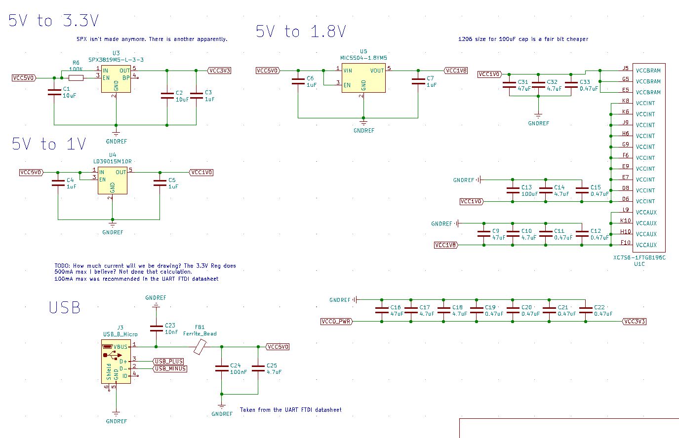
I use KiCAD for my designs. It's not a bad piece of software and I've not had too many problems with it. Sadly, it doesn't have great support, if any, for reusing schematics. I've just about gotten my head around the libaries for footprints and components but I'd really like to cut and paste between designs.
The FPGA itself is a complex component. It has many pins, organised into various banks. I couldn't find a component or footprint online, so I made my own. The component itself is broken up into subcomponents - KiCAD allows this feature which is nice. It means I can have the FPGA appear on multiple sheets, but only the bits of the FPGA that are relevant to that sheet. It keeps things neat.
There aren't too many other components on our first board. There's a footprint for some memory - SRAM in this case. SRAM requires very little in the way of circuitry. There's a USB to UART chip which again, is relatively straight forward. What wasn't so easy is finding the chip with the right footprint. I intended to hand solder this part, but unfortunately, we were caught out by the worldwide chip shortage. We managed to source a few in the end but it took a bit of doing.
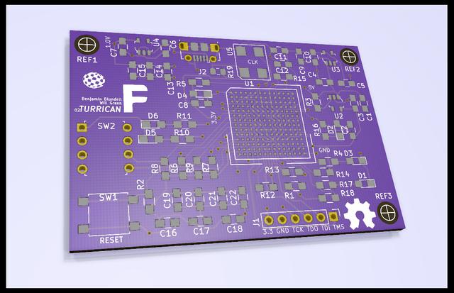
Finally, there is the Pmod connector. This is a standard setup by Digilent, an FPGA manufacturer, used for peripherals. I managed to find some footprints for the sockets.
FPGAs are all Ball Grid Array packages, or BGA. This means that rather than pins or legs, they has small solder balls on the underside of the package. The only way to attach this to a board is to bake it in a reflow oven. This is the way most electronics are assembled these days.
The proper way is to pay a manufacturer to build it all for you. You design your board with robots in mind, send it off to a board house with a big pick-and-place machine and a large oven. Job done. However, this costs a lot and is really only done for big orders. BGA presents a bit of a blocker to the hobbyist.
Fortunately, there are loads of cheap or hacked solder ovens out there. If you live in the USA you might be familiar with the toaster oven. Apparently, they can make great reflow ovens. If you are in the UK and have been to EMF, you might be interested to know that the badges have in the past, been made by placing the boards over an oven stove. I've tried this latter tactic before and it didn't work for me, but I'm told it can work.
In the end, I bought a cheap solder oven - the hackers favourite T962A reflow oven. It's apparently far from ideal but so far, I've not had any real trouble with it.
When reflowing solder, you need to use some solder paste. This grey, viscous stuff is full of tiny balls of solder. When heated, it'll melt and flow - capillary action doing the rest. But it needs to be applied to the pads on the PCB first. The correct way to do this is with a metal stencil. However, these are quite expensive.
I managed to find a supplier in the UK who would laser cut mylar sheets instead - Hobbytronics. Mylar isn't great but for a single component, it's not too bad. I decided I'd just reflow the FPGA - keep it simple. I could hand-solder the rest easily enough. I cut some plastic from an old curry tub, squirted on the paste over the mask, then scraped the paste over the holes. Carefully removing the mask, the solder seemed to go exactly where I wanted it.
One tip I've learned with this method - if you are using mylar always use circles in your mask. Never laser cut small rectangles, close together. The thin mylar doesn't hold up to the scraping and the paste goes everywhere.
The nerve racking bit is placing the FPGA on top of the solder before baking. I've tried using tweezers and the like, but in the end, I've just used my fingers. If I think it's gone wrong, I'll remove it, wipe it all down carefully and start again. I've not had to do that too many times yet - the outline on the PCB really helps.
I found that an inverted 'V' shape on the temperature graph worked well for reflowing the FPGA. The datasheet lists the recommended curves and temperatures and this one seemed the closest.
So far, this technique has worked four times in a row - not too shabby!
Most of the components are 2012 (0805 in old money). I'm pretty comfortable hand soldering these. Typically, I dab solder on one pad, place the component while melting the solder, let it set, then solder the other pad. Larger components often require the solder, flux, solder-braid three step. The idea here is you coat all the legs with solder, then wick off the excess. This works really well, but it's not always perfect. I've had several joints that looked right at first glance, but were in fact not connected. It pays to check and check again. I use a hacked loupe I snaffled out of a photocopier to get a closer look.
I tend to work methodically, working down the BOM in order. Some folks say it's best to start with the larger components as they need more heat. This is also good advice I think. I use a scalpel to open the tiny packaging slowly, so as not to have the tiny components ping out all over the place. A pair of good tweezer is also essential for getting the parts in place.
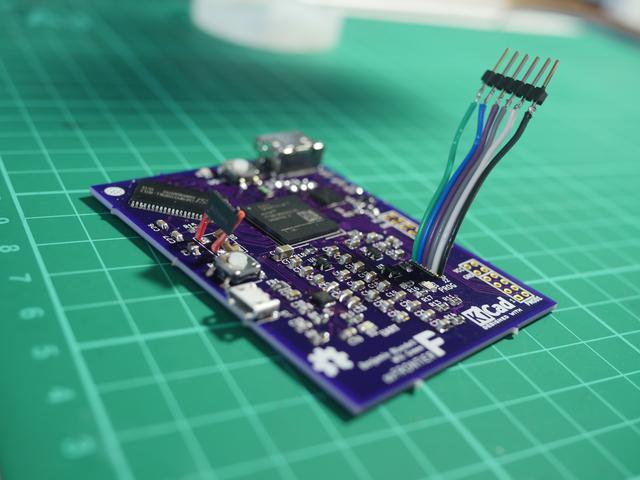
There's always a risk of mistakes when working on a project like this. On this board, I got the footprint for the oscillator the wrong way around! I also used the wrong pitch for the JTAG connector. Silly me! Still, these things happen and learning to work around them seems to be a useful skill.
So with everything soldered in place, tested and found to be working, we can program our FPGA with a little JTAG cable. The first thing we do is flash an LED, because of course you do! Using Xilinx's Vivado we can build our little design, flash it to the FPGA and pray.
Once I got the flashing LED going, the next step was to try some VGA. Video Graphics Array is an old technology but it seems fairly robust. It's analog and so requires a few more components. Fortunately, the Digital-to-Analog part can be taken care of by a VGA Pmod from Digilent. This cute little board just slots into the two Pmod connectors on our board. All that's left is to generate the correct digital signals.
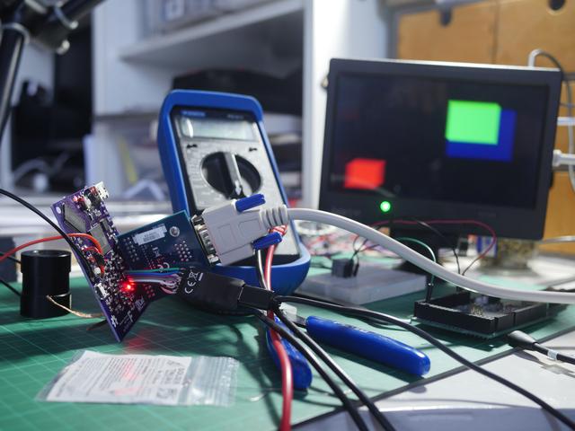
Fortunately, Will has been hard at work on this for a while. Checkout his amazing series on FPGA graphics. It's pretty much the best out there (I mean I would say that, but it totally is!). Using his code, we can flash our FPGA and POW! Funky, animated squares! Job done!
FPGAs are quite amazing bits of kit. Hardware is hard though, and although we can design a lot of it in software, there is still so much to do that can go wrong. I've not spoken too much of the mistakes I've made or the problems I've overcome. This is common in any electronics project, but FPGAs are somewhat tricky in that they are somewhat opaque in terms of hardware debugging, at least for me. Once it's soldered on, that's it! You can't get a test probe on there, or remove it and try again (at least not easily). Even if you could get a probe onto it to test the signals, many of the kinds of signals FPGAs deal with a super fast - super high bandwidth. I've yet to find a scope that can look at HDMI signals for instance (I'm sure they exist but they are probably super expensive!).
In the end though, we now know how to get the basics. There's more to look at, such as the memory, peripherals, sound and better visuals, but hardware takes time. It's worth it though, when it finally works!